Skip to content
  • English
  • Business
  • Entertainment
  • National
  • Lifestyle
  • Education
Daily News India

Daily News India

Just another WordPress site

  • English
  • Business
  • Entertainment
  • National
  • Lifestyle
  • Education
  • Toggle search form
  • Building Future-ready Workforce To Bridge The Great Indian Skill Gap Business
  • Highbar Technocrat Limited Wins Prestigious SAP Net New Business Partner of the Year 2024 Award Business
  • Tetra Pay (TPAY) Token – A Massive Breakthrough in Cryptocurrency Business
  • Mumbai hosts launch of A City Called Agroha, the first full reconstruction of Samrat Agrasen’s ancient republic Lifestyle
  • Celebrities Who Swear by Cranberries – Here’s Why Health
  • Morzze Showcases Innovation at INTEXT EXPO 2025 with the Launch of MFD 1101 Food Waste Disposer Business
  • Top 7 Restaurant Furniture Manufacturers in India Business
  • Arshi Ghosh wins the Miss Transqueen India 2023 pageant held in New Delhi Lifestyle

RRP Electronics Ltd Launched Maharashtra’s First OSAT/ATMP Semiconductor Manufacturing Facility

Posted on September 19, 2024 By

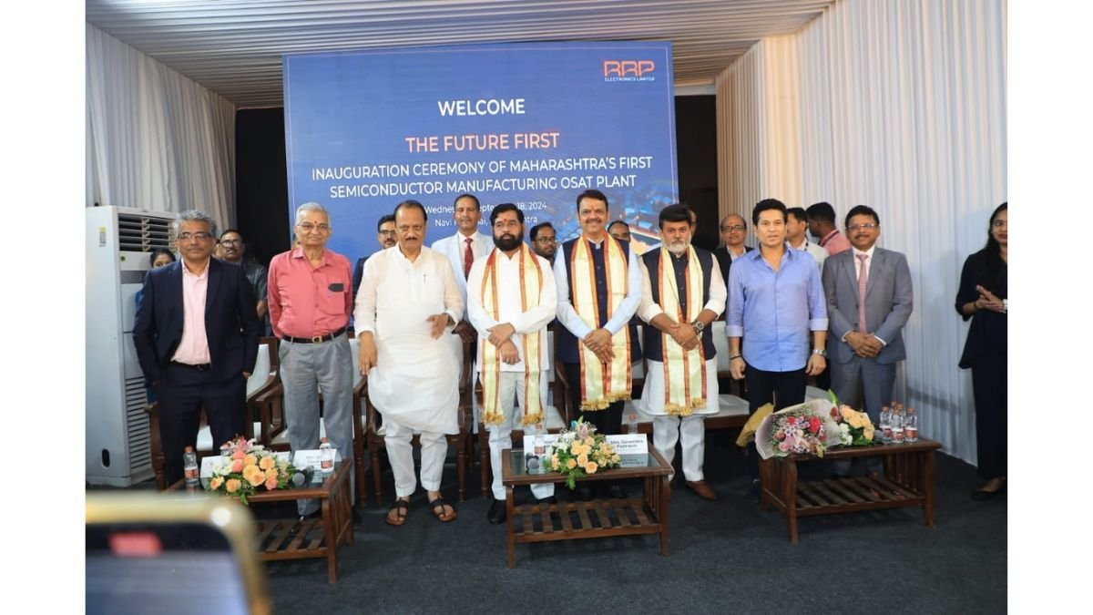
Mumbai (Maharashtra) [India] September 19: RRP Electronics Ltd was pleased to announce the launch of Maharashtra’s first OSAT (Outsourced Semiconductor Assembly and Test)/ATMP (Assembly, Testing, Marking, and Packaging) semiconductor manufacturing facility in Navi Mumbai, marking a major milestone in India’s semiconductor mission.

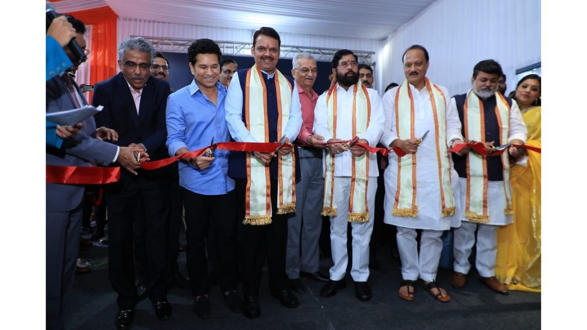
The inauguration was led by Shri Eknath Shinde, Honorable Chief Minister of Maharashtra; Shri Devendra Fadnavis, Deputy Chief Minister; and Shri Ajit Pawar, Deputy Chief Minister of Finance. The event also saw the presence of Shri Uday Samant, Minister of Industries; Dr. Harshdeep Kamble, Principal Secretary of Industries, Government of Maharashtra; Bharat Ratna awardee and renowned cricketer Sachin Tendulkar; and Dr. Anil Kakodkar, Padma Vibhushan awardee and former Chairman of the Department of Atomic Energy.

RRP Electronics Ltd

Supported by a strong technological partnership with HMT Microelectronic AG and its leading associates, this facility was set to redefine the semiconductor landscape. It was equipped to handle advanced packaging technologies such as QFN, BGA, SoC, and mixed ASICs.

In its initial phase, the facility had the capacity to produce 10,000 wafers per month. Future plans included the establishment of a dedicated design house and expansion into LiDAR technology development, addressing the growing demand for automotive power chips, as well as the production of TFT and WATN components for automotive applications.

An MoU was signed between HMT Microelectronic AG and Renowa Vision Inc. The MoU with HMT symbolized projects related to QFN, BGA, ASICs, and later expansion into LiDAR technology. The MoU with Renowa marked a significant leap in RRP’s growth journey, as it allowed the acquisition of technology for OSAT and FAB for NAND memory chips. These are non-volatile storage technologies that do not require power to retain data.

The signing of these MoUs provided RRP with assured revenue generation of over $50 million in the OSAT sector.

This groundbreaking project represented a significant achievement for Maharashtra, further positioning the state as a key player in India’s semiconductor mission.

If you have any objection to this press release content, kindly contact pr.error.rectification@gmail.com to notify us. We will respond and rectify the situation in the next 24 hours.

Technology Tags:technology

Post navigation

Previous Post: Making Every Occasion Extra Special with Gifting Studio
Next Post: Hafele’s Sanctus Shower Cubicle

Related Posts

  • Panjab University Collaborates with ISAC and Zscaler to Establish CopConnect Cyber Wellness Clinic Technology
  • The Hidden Drain: Why Manual IT Asset Handoffs Are Costing Companies More Than They Realize Technology
  • A Legacy of Innovation: The Evolution of Aiinhome Technologies Technology
  • When Machines Start Consuming Cities: xAI’s Colossus, Ambition, And The Price Of Thinking Faster Technology
  • LUCID’s customised implants to address facial deformities in Mucormycosis patients Technology
  • ISRO Chief Somanath unveils Zero Emission initiative of SFO Technologies Technology

Recent Posts

  • How to Stop Hair Fall in Winter: Real Reasons, Real Fixes, No Nonsense
  • BGMI Releases Redeem Codes Featuring Casual Stroll Set and In-Game Rewards
  • Why Indian Students at MIT University Sikkim Are Prioritizing Skills Along with Degrees
  • 5 Leading Shilajit Brands in India (Authoritative 2026 Report)
  • SATCON 2026 wraps up in Delhi with 250+ delegates from 7 countries

Recent Comments

  • Unknown on Participants Reap Rewards in Wellman’s 8-Week Digital Campaign: IPL Tickets, Autographed Virat Kohli Merchandise, and More!
  • How Dr. Mohammad Baydoun Became the Vice President of Development at Damac Properties Business
  • Revolutionizing Baby Care: A Step into Eco-conscious Future of Diaper Technology Business
  • Indian Startup Astberg Tackles ‘Silent Killer’ of Indoor Air Pollution with Cutting-Edge Tech Business
  • How Rustom Kerawalla’s VIBGYOR World Academy is preparing students with a One World Vision Education
  • Teestar® Bioactive Gummies by Avesthagen Limited Business
  • Tidbits, a standout performer in the Indian E-Commerce Food platform! Business
  • Lakhs of couples are getting hope of parenthood through this IVF centre! Lifestyle
  • Mast Banarasi Paan: India’s First and Fastest-Growing Tobacco-Free Paan Franchise Expands to 400+ Outlets Business

Copyright © 2026 Daily News India.

Powered by PressBook News WordPress theme